
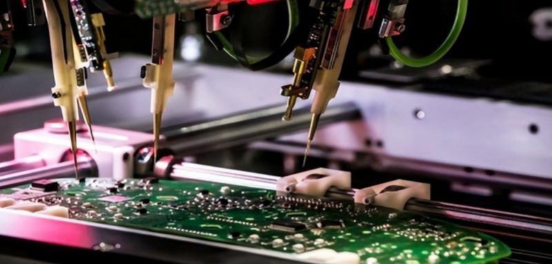
Printed Circuit Board (PCB) manufacturing requires rigorous testing to ensure functionality, reliability, and performance. Without proper testing, defects can lead to costly failures. This guide explores 7 crucial PCB testing technologies, their pros and cons, and best practices to optimize your manufacturing process.
1. What is Design for Test (DFT) in PCB Manufacturing?
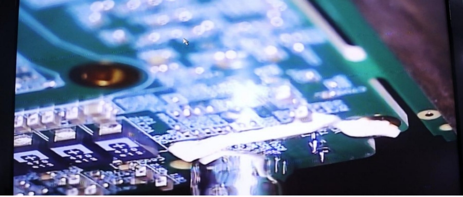
Design for Test (DFT) is a methodology that ensures PCBs can be effectively tested for defects after assembly. Unlike Design for Manufacturability (DFM), which prevents issues before production, DFT focuses on detecting problems during manufacturing through techniques like:
X-ray Inspection
Automated Optical Inspection (AOI)
- In-Circuit Testing (ICT)
Functional Circuit Testing (FCT)
Key Objectives of DFT
✔ Verify PCB design accuracy
✔ Detect manufacturing defects (shorts, opens, misalignments)
✔ Ensure all components function correctly
Common DFT Challenges
Improper component spacing
Incorrect solder mask application
Suboptimal drill sizes
Faulty surface mount pads
Acid traps (etching flaws)
2. Critical Parameters in PCB Test Design
To enhance testability, engineers must consider:
✅ Test Points – Improve probe access for efficient testing.
✅ Test Traces – Allow signal behavior analysis via oscilloscopes.
✅ Debug LEDs – Indicate power status in microcontrollers/FPGAs.
✅ Connectors & Vias – Enable voltage measurements and continuity checks.
3. Two Fundamental PCB Testing Phases
A. Bare Board Testing
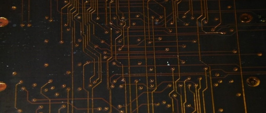
Conducted before component assembly to check:
Continuity (ensures no open circuits)
Isolation (verifies no unintended connections)
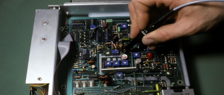
B. Assembled Board Testing
Performed after component placement to validate:
Solder joint integrity
Component functionality
4. 7 Essential PCB Testing Technologies
1. Flying Probe Test
How It Works: Movable probes test components without fixtures.
Best For: Low-volume production, prototype testing.
Pros:
No custom fixtures needed
High test coverage
Cons:
Slower than ICT
Limited for high-volume production
2. In-Circuit Test (ICT)
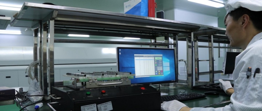
How It Works: Uses fixed probes to check electrical performance.
Best For: Mass production.
Pros:
Fast & accurate (90%+ coverage)
Detects shorts, opens, and faulty components
Cons:
Expensive fixtures
Not ideal for small batches
3. Functional Circuit Test (FCT)
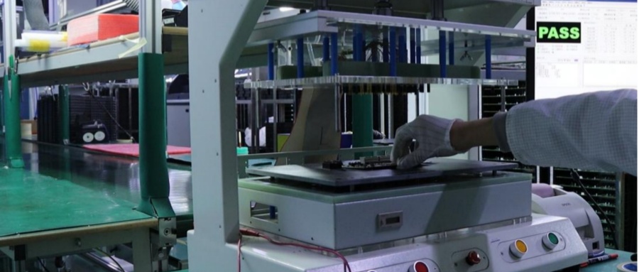
How It Works: Simulates real-world operation.
Best For: Final validation before shipment.
Pros:
Low-cost & customizable
Ensures end-product functionality
Cons:
Requires skilled technicians
4. Automated Optical Inspection (AOI)
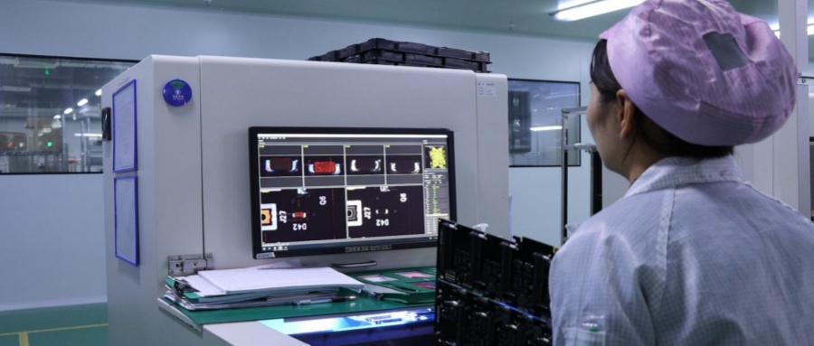
How It Works: Cameras compare PCBs against reference designs.
Best For: Detecting surface defects (solder bridges, missing parts).
Pros: High precision for visible flaws
Cons: Cannot inspect hidden connections
5. Aging Test (Burn-In Testing)
How It Works: Stresses PCBs beyond normal conditions to find early failures.
Best For: High-reliability applications (medical, aerospace).
Pros: Identifies weak components
Cons: Shortens PCB lifespan
6. X-Ray Inspection
How It Works: Reveals hidden defects in BGAs, vias, and internal layers.
Best For: Complex, high-density PCBs.
Pros: Non-destructive internal inspection
Cons: Expensive & requires expertise
7. Manual Visual Inspection (MVI)
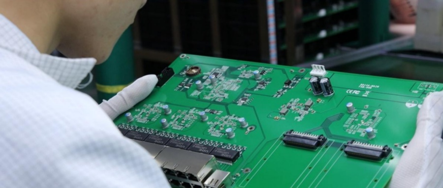
How It Works: Technicians examine PCBs under magnification.
Best For: Quick checks of obvious defects.
Pros: Simple & cost-effective
Cons: Human error risk
5. 9 Best Practices for Effective PCB Testing
Maintain Clear Board Edges – Ensures proper fixture alignment.
Use Fiducial Markers – Helps machines locate test points accurately.
Leave Vias Uncovered – Allows probe access for testing.
Place Probes Near Component Legs – Detects solder joint issues.
Cluster Test Points – Speeds up testing in large PCBs.
Clean Flux Residues – Prevents false test failures.
Include Power/Ground Probe Points – Simplifies short-circuit detection.
Maximize Single-Side Testing – Reduces costs by avoiding double-sided fixtures.
Control Component Height – Prevents probe interference.
Conclusion: Optimize PCB Testing for Quality & Cost Efficiency
Effective PCB testing minimizes defects, improves yield, and reduces manufacturing costs. Combining AOI, ICT, and FCT ensures comprehensive coverage, while DFT principles enhance testability from the design stage.