
Introduction: Understanding PCB Production
Printed circuit board (PCB) manufacturing is a complex but structured process that transforms raw materials into functional boards. Whether you’re an engineer, designer, or electronics enthusiast, understanding how PCBs are made helps in selecting the right manufacturer and ensuring quality.
In this guide, we’ll break down the single-layer, double-layer, multi-layer, and HDI PCB manufacturing processes, highlight key differences, and explain industry variations.
1. Single/Double-Layer PCB Manufacturing Process (13 Steps)
Single and double-layer PCBs are the simplest and most cost-effective. Here’s how they’re made:
Key Steps in Single/Double-Layer PCB Production
-
Material Cutting – Copper-clad laminates are cut to size.
-
Drilling – Holes for components and vias are drilled.
-
Copper Deposition – Electroless copper coats hole walls for conductivity.
-
Electroplating – Additional copper strengthens connections.
-
Pattern Transfer – UV exposure transfers circuit design onto the board.
-
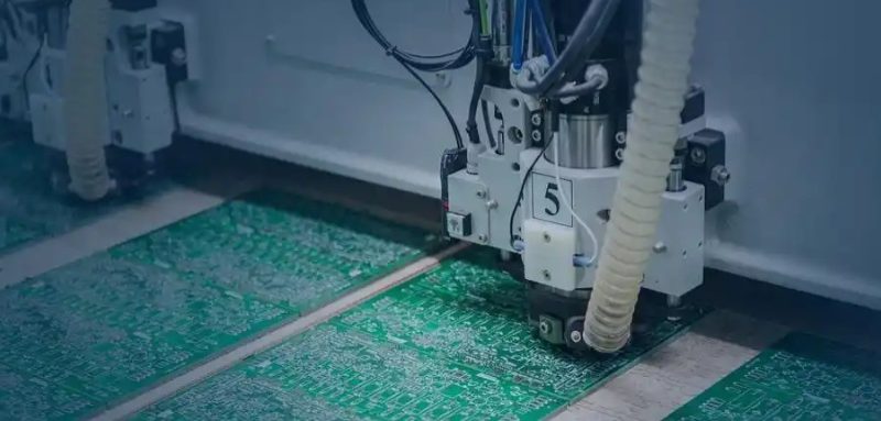
AOI Inspection (AOI) – Automated optical inspection checks for defects.
-
Solder Mask Application – Protective layer prevents short circuits.
-
Silkscreen Printing – Labels and markings are added.
-
Surface Finish – Coatings like HASL, ENIG, or OSP prevent oxidation.
-
Electrical Testing – Ensures all connections work.
-
Routing & V-Cutting – Boards are cut to final shape.
-
Final Quality Check (FQC) – Manual inspection before shipping.
-
Packaging – Safe packing for delivery.
Best for: Simple electronics, prototypes, low-cost projects.
2. Multi-Layer PCB Manufacturing Process
Multi-layer PCBs (4+ layers) are used in advanced electronics like smartphones, servers, and medical devices.
Key Differences from Single/Double-Layer PCBs
-
Inner Layer Processing – Additional steps for bonding layers.
-
More Lamination & Inspection Stages – Ensures layer alignment and reliability.
Critical Steps in Multi-Layer PCB Production
-
Inner Layer Imaging – Circuit patterns etched onto inner layers.
-
AOI Inspection (AOI) – Checks inner layers for defects.
-
Brown Oxidation – Improves adhesion before lamination.
-
Lamination – Heat and pressure bond layers together.
-
Laser Drilling – Precision holes for microvias.
-
Plating & Electroplating – Ensures conductivity in vias.
-
Outer Layer Imaging – Final circuit pattern transfer.
-
Final Testing & Finishing – Same as single/double-layer PCBs.
Best for: High-performance electronics, compact designs, IoT devices.
3. HDI PCB Manufacturing (Advanced Process for High-Density Designs)
HDI (High-Density Interconnect) PCBs are used in smartphones, wearables, and aerospace tech.
Key Features of HDI PCBs
✔ Laser Microvias – Smaller, more precise holes.
✔ Multiple Lamination Cycles (N-1 Pressing) – Ultra-thin layers.
✔ Sequential Build-Up (SBU) Technology – Higher circuit density.
Best for: Miniaturized, high-speed electronics.
4. PCB Manufacturing Variations (MI – Manufacturing Instructions)
Even with the same design, manufacturers may adjust:
-
Hole Metallization: Copper sinking vs. “black hole” process.
-
Surface Finishes: HASL (cheap), ENIG (reliable), or Immersion Silver (high-frequency).
-
Testing Methods: Flying probe vs. fixture-based testing.
Pro Tip: Always discuss MI (Manufacturing Instructions) with your PCB supplier to avoid surprises.
5. How to Choose the Best PCB Manufacturer
When selecting a PCB supplier, look for:
✅ Experience with Your PCB Type (HDI, flex, rigid-flex, etc.)
✅ Quality Certifications (ISO, UL, IPC standards)
✅ Fast Turnaround & Reliable Testing (AOI, impedance control)
✅ Environmental Compliance (RoHS, REACH)
Why FuxinPCBA?
✔ High-reliability multi-layer PCBs
✔ Quick turnaround & competitive pricing
✔ Full testing & inspection for defect-free boards
Conclusion: PCB Manufacturing Made Simple
Understanding the PCB production process helps in:
✔ Selecting the right PCB type for your project.
✔ Communicating effectively with manufacturers.
✔ Ensuring high-quality, reliable boards.
Need PCBs manufactured? Choose a supplier that follows strict quality control and offers the right capabilities for your design!