
FuxinpcbaKey Takeaways:
✅ *Early Boundary Scan integration cuts test development costs by 30-50%*
✅ Reusable tests across ICT/FT stations streamline manufacturing
✅ Achieve >95% digital interconnect coverage
Why PCBA Testing Efficiency Matters
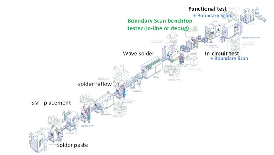
For OEMs and contract manufacturers (CMs), PCBA testing costs directly impact competitiveness. With defects potentially introduced at SMT placement, reflow soldering, or functional validation stages (Fig 1), comprehensive testing is non-negotiable.
Core PCBA Testing Stages
| Test Stage | Purpose | Defects Detected |
|---|---|---|
| ICT (In-Circuit Test) | Verify component values, opens/shorts, power-on functionality | Faulty components, soldering defects |
| FT (Functional Test) | Validate board-level operational performance | Functional block failures |
| Repair Stations | Correct ICT/FT failures | Component/Soldering rework |
Boundary Scan: The Game-Changer for DFT
Boundary Scan Testing (IEEE 1149.1) revolutionizes Design for Testability (DFT) by embedding test access into digital ICs.
How It Works
-
Scan Cells: Shift registers between device pins and internal logic (Fig 2)
-
Control & Observation: Test signal integrity at every pin
-
Interconnect Testing: Validate connections between boundary scan devices
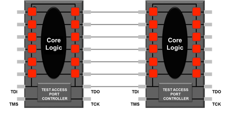
Fucxinpcba Boundary scan and interconnect test implementation on the device
Key Advantages
-
Tests non-boundary scan devices (DDR, Flash, EEPROM)
-
Executes Built-In Self-Test (BIST) via BSDL
-
Eliminates up to 70% physical test points
“Implementing Boundary Scan at prototype stage reduces NPI delays by 40%” – Industry Analysis
Phased Implementation for Maximum ROI
Phase 1: Prototype Design [Critical for DFT Success]
-
Verify testability before board assembly
-
Identify nets requiring Boundary Scan vs ICT
-
Reduce structural defects risk
Phase 2: New Product Introduction (NPI)
-
Reuse pre-validated Boundary Scan tests
-
Cut ICT development time by 30%
-
Lower fixture costs with fewer test points
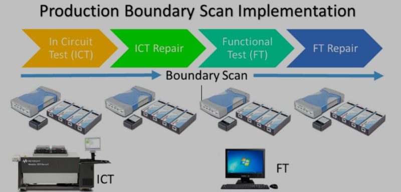
Phase 3: Mass Production (Fig 3)
-
Unified Testing: Same Boundary Scan tests at:
-
ICT stations
-
Functional test (FT) stations
-
Repair stations
-
-
Cost Savings: Hardware/software reuse across sites
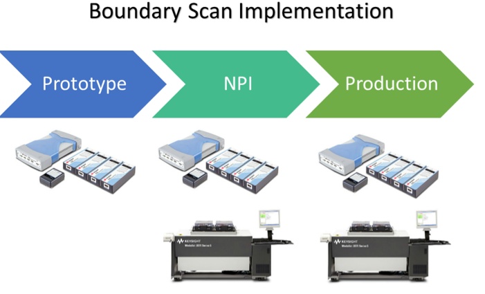
Fuxinpcba Boundary Scan Implementation from Prototype (Design Phase) to New Product
4 Strategic Benefits of Boundary Scan
-
Cost Reduction
-
50% lower test development costs
-
35% fixture cost savings
-
-
Enhanced Coverage
-
Near-complete digital interconnect validation
-
-
Faster Time-to-Market
-
30% shorter NPI phases
-
-
Repair Efficiency
-
Standardized diagnostics across test stages
-
Conclusion: Building a Future-Proof Test Strategy
Integrating Boundary Scan testing from prototype to production delivers:
-
Lower capital expenditure on test hardware
-
Higher first-pass yields
-
Reduced technician training time
Electronics manufacturers leveraging this approach report 22% faster ROI on test investments.
Ready to optimize your PCBA test process? [Contact Us for DFT Consultation]
Recent Comments