

What is PCBA Testing?
PCBA testing refers to the detection and evaluation of the pcb assembly board. Including the IC burning,components checking,functional testing. With the testing, Pcb assembly manufacturer can assure and meet your quality requirements,before products are delivered.
The Importance of PCBA Testing
The printed circuit board (PCB) is very important for electronic information products because it holds the components and lets signals move through the circuits. The quality of the PCB affects how good and reliable the final product is. To follow the rules about the environment and avoid problems like not enough solder, cracks, and layers coming apart, it’s really important to test the PCB assembly (PCBA) at the right time.
To make sure the PCB is good and reliable, manufacturers have to check it at different times during the making and assembly process. This helps them find and fix problems on the surface. It also helps them control the process by collecting information and finding problems before they test the electrical parts.
Because surface mount devices need stronger connections than the older through-hole technology, it’s extra important to test PCBAs that use surface mount technology (SMT). If there’s not enough solder, the parts won’t stay attached well, and the PCB won’t work reliably for a long time. This shows how important it is to test the PCBAs to make sure the solder connections are strong.
PCBA Testing Methods
-
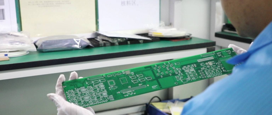
Visual Inspection
Visual inspection is used in the PCBA manufacturing process at different stages. Inspectors visually identify obvious defects such as contaminated solder paste and missing components after solder paste printing and component placement. The most common method involves examining the reflow solder joints by observing the light reflected from ordinary prisms at different angles. This inspection can test 5 joints in just one second.
The effectiveness of visual inspection depends on the skills of the inspector and the consistency and applicability of inspection standards. Inspectors must understand the technical requirements for each type of solder joint, as there may be up to 8 defect criteria for each type, and different assembly equipment may have more than 6 types of solder joints. However, visual inspection is not suitable for precise measurements for effective process control. It is also not applicable for inspecting hidden solder joints, such as J-lead devices with high-density packaging, ultra-fine square flat devices, surface mount inverted chip devices, or BGA (Ball Grid Array) devices. Nevertheless, visual inspection is a low-cost and easily accessible technology suitable for detecting significant defects based on established and specific rules.
-
Structure Process Testing System (SPTS)
The Structure Process Testing System (SPTS) is an automated system that digitizes and analyzes video capture in real-time. It greatly improves the accuracy and consistency of visual inspection. SPTS uses different types of light, such as visible light, laser beams, and X-rays, to gather information. It processes images to detect and measure defects related to the quality of solder joints.
Like visual inspection, SPTS doesn’t require physical contact with the circuit board. However, unlike visual inspection, it provides high consistency and removes the subjective nature of defect measurement.
-
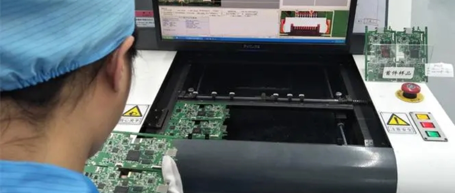
Automatic Optical Inspection (AOI)
The AOI system uses lights, programmable LEDs, and cameras to shine light on solder joints and capture images. The leads and solder joints reflect the light, while the PCB and SMD reflect very little. By analyzing the shape and intensity of the reflections, experts can assess the quality of the solder joints, the adequacy of the solder, and the presence of any issues like poor wetting, solder bridging, missing components, or displacement.
AOI equipment is fast, inspecting 30-50 joints per second, and cost-effective. However, it cannot measure solder joint height or check if there is solder inside the joints. It also cannot inspect hidden solder joints, which are important for reliable soldering in certain types of devices. In conclusion, AOI testing works best for inspecting ICs and gull-wing devices with a spacing greater than 0.5mm.
-
Automatic Laser Testing (ALT) Measurement
ALT is a technique used to test the height and shape of solder joints or solder paste deposits. The system measures the height and reflectivity of specific surface components by focusing the laser beam’s image on one or more position-sensitive detectors held at a specific angle relative to the laser beam. During ALT measurement, the surface height is determined by the position of the reflected light, while the surface reflectivity is calculated from the power of the reflected beam.
The beam may illuminate multiple positions of the detectors due to secondary reflections, so a method is needed to distinguish the correct measurements. Additionally, the reflected beam may encounter shielding or interference from obstructing materials as it travels along the detector. To address these issues, the system tests the reflected laser beam along an independently adjusted optical path to eliminate multiple reflections and prevent shielding.
The ALT system OPTIMAL is used for measuring the heights of solder joints, as well as solder paste deposition and component alignment before assembly. It provides real-time process control data for solder paste printing, including viscosity, alignment, cleanliness, flowability, extrusion speed, and stress.
-
X-ray Fluorescence Inspection System
The X-ray fluorescence inspection system utilizes a single light source to emit a beam through the circuit board. Solder joints cause a greater reduction in light intensity compared to other materials. This difference in light energy is converted into a grayscale X-ray image with 256 levels. These grayscale images display the thickness, distribution, and integrity of the solder joints.
For single-sided PCBs, the X-ray fluorescence inspection system accurately identifies solder joint defects. These defects may include cracks, insufficient solder, bridging, misalignment, gaps, and more. It can also detect missing components and reverse tantalum capacitors. However, it cannot effectively detect defects on double-sided PCBs due to the overlapping X-ray images of solder joints on both sides of the board.
-
X-ray Laminography System
Compared to X-ray fluoroscopy systems, X-ray laminography systems generate horizontal cross-sectional images of the focal plane by scanning or rotating synchronously with the X-ray detector. Off-axis images on the detector are then used to create cross-sectional images with a surface thickness of 0.2-0.4mm through single or multiple swings, resulting in homogenization. This allows for distinguishing solder joints within the focal plane from other materials on the PCB.
X-ray laminography systems use a laser rangefinder to determine and correct the surface position of the board relative to the focal plane, compensating for board warpage. The circuit board is then incrementally moved vertically in small increments to pass through the focal plane, enabling inspection of different portions of the same solder joints. This system is suitable for inspecting BGA and PTH solder joints. For double-sided PCBs, they are vertically moved in large increments to pass through the focal plane and inspect solder joints on both sides.
The X-ray laminography system allows for adjusting the scanning radius of the beam and the vertical movement of the focal plane, enabling different magnification factors or visual field sizes to be set. This system can measure parameters of all physical solder joints on different focal planes, providing coverage for process defects. By analyzing the measurement results, data will be provided for characterization and assembly improvement.
PCBA Testing and Inspection procedure
PCBA testing encompasses various techniques, each serving a specific purpose in evaluating the quality and functionality of the printed circuit board assembly. Let’s explore the related procedure:
-
Firmare Programming
After the PCBA board is completed the front-end welding process, the engineer starts to program the single-chip microcomputerin the PCBA board, so that the single-chip microcomputer can realize specific functions.
-
ICT(In-Circuit Testing)
In-circuit testing uses a software-operated machine to place the PCB on a set of spring-loaded pins. This method detects faults such as shorts or opens in the circuit and measures resistance and capacitance. However, it may be expensive due to the need for different fixtures for PCBs with different designsThe FCT test can test the environment, current, voltage, pressure and other parameters of the PCBA. The test content is relatively comprehensive, which can ensure that various parameters of the PCBA board meet the design requirements.
-
FCT (Functional Testing)
Functional testing simulates the operating environment of the PCB to evaluate its performance. It is performed in the final phase of production and does not require specialized equipment in most cases. However, FCT is not a stress test, and the PCB may still fail under extreme conditions.
-
Burn-in Testing
Burn-in testing involves subjecting the PCB to extreme conditions, such as high temperatures and voltages, to identify any operational errors. This stress test helps engineers identify potential issues and ensures the reliability of the PCB. However, it can be time-consuming and may shorten the PCB’s lifespan.
Conclusion
PCBA testing is a crucial step in ensuring the quality and functionality of pcbas,manufacturers can detect and prevent defects, saving time and resources and ensuring customer satisfaction.After the PCBA pass a series of tests, the qualified PCBA board can be labeled with a qualified label, and finally packaged and shipped.
About Fuxin
At Fuxin, we prioritize the quality by employing strict PCBA testing producre. Our commitment to a reliable and efficient testing process ensures that our products meet or exceed your quality requirements. Trust us as your EMS partner, and experience the difference of working with a manufacturer dedicated to delivering excellence.