
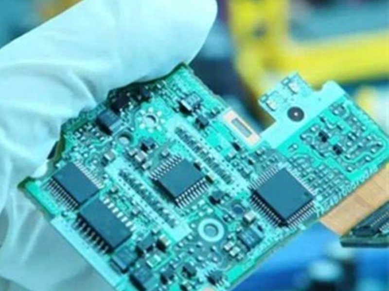
High-quality PCB assembly (PCBA) is now a crucial requirement in the electronics industry. PCBA serves as the integrated component of various electronic devices. If PCB component manufacturers fail to perform operations accurately due to manufacturing errors, it can compromise the functionality of electronic devices. To mitigate these risks, PCB and assembly manufacturers are implementing different inspection techniques at various manufacturing steps to ensure the quality of PCBA..
PCBA Inspection Methods
Nowadays, identifying manufacturing defects in printed circuit boards (PCBs) has become increasingly challenging due to their increasing complexity. Common defects found in PCBs include open circuits, short circuits, incorrect orientations, inconsistent soldering, misaligned components, misplaced components, defective non-electrical components, missing electrical components, and more. To prevent these situations, turnkey PCB assembly manufacturers employ the following inspection methods.
All the techniques discussed above ensure accurate inspection of electronic PCB components and help ensure their quality before leaving the factory. If you are considering PCB assembly for your next project, make sure to source from a reliable PCB assembly service.
First Article Inspection
The production quality always depends on the smooth operation of Surface Mount Technology (SMT). Therefore, before starting mass assembly and production, PCB manufacturers perform a first article inspection to ensure the correct installation of SMT equipment. This inspection helps them detect issues with vacuum nozzles and alignment, which can be avoided in mass production.
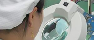
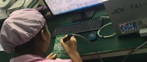
Visual Inspection
Visual inspection, which is also referred to as naked-eye inspection, is a widely used technique in the processes of PCB assembly. This technique involves the examination of components using either the human eye or detectors. The choice of equipment utilized for this inspection depends on the specific area that is being examined. For instance, visible component placement and solder paste printing can be inspected by relying on the naked eye. However, the assessment of solder paste deposition and copper pads necessitates the use of a Z-height detector to uncover any potential issues. One of the most commonly employed methods of visual inspection is carried out at the reflow solder joint, where a prism is utilized. This prism analyzes the reflected light from various angles, enabling the detection of any existing defects.
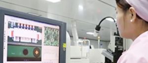
Automated Optical Inspection (AOI)
AOI (Automated Optical Inspection) is the most common and comprehensive method used for visual inspection to identify defects. This method typically utilizes multiple cameras, light sources, and a programmed LED library. AOI systems can capture images of solder joints and tilted components from different angles, allowing them to inspect 30 to 50 joints per second. This significantly reduces the time required for defect identification and correction. Nowadays, AOI systems are utilized at various stages of PCB assembly.
In the past, AOI systems were not considered ideal for measuring solder joint heights on PCBs. However, the emergence of 3D AOI systems has made this capability possible.
Recently, advancements in 3D AOI systems have made it possible to accurately measure solder joint heights on PCBs. This capability has greatly improved the inspection process and ensures the quality of PCB components before they leave the factory. In addition, AOI systems are highly effective in inspecting components with complex shapes and a spacing of 0.5m.
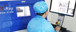
X-ray Inspection
The demand for PCB components with denser and more compact sizes is increasing due to their use in miniature devices. Surface Mount Technology (SMT) has become a popular choice among PCB manufacturers for designing dense and complex PCBs with BGA package components. While SMT helps reduce the size of PCB packages, it also introduces complexities that are not visible to the naked eye. For instance, a small Chip Scale Package (CSP) created using SMT may have around 15,000 solder connections, making it difficult to verify them visually. This is where X-ray technology comes into play. X-ray has the ability to penetrate solder joints and detect missing solder balls, solder positions, misalignments, and more. It can penetrate the chip package, which is closely connected between the circuit board and the solder joints below.
At Fuxin we believe that we earn your continuous trust as your reliable partner for EMS by always delivering products that meet or exceed your quality requirements. We employ a strict Quality Management System (QMS) to control the whole production process, so that quality is assured at every level of assembly.