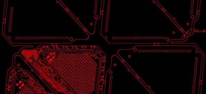
Why PCB Panelization Matters
Printed Circuit Board (PCB) panelization is a crucial step in electronics manufacturing. By arranging multiple smaller PCBs into a single panel, manufacturers can:
✅ Reduce production costs
✅ Improve assembly efficiency
✅ Minimize material waste
✅ Enhance structural stability during soldering
In this guide, we’ll cover best practices for PCB panelization, including design considerations, connection methods, and real-world examples to optimize your manufacturing process.
1. PCB Panelization Design: Key Considerations
When designing a PCB panel, focus on:
✔ Panel Layout Optimization
-
Material Efficiency – Arrange sub-boards to minimize waste.
-
Structural Rigidity – Prevent warping during wave soldering.
-
Easy Depaneling – Ensure clean separation post-assembly.
✔ Recommended Panel Sizes
-
Ideal dimensions should match final assembled size (see industry standards).
-
Oversized panels (>300mm) may cause SMT machine slowdowns (see Figure 1).
✔ Common Panelization Strategies
① For Large PCBs (Long Side ≥125mm)
-
Use V-groove panelization (Figure 7a) for rigidity.
-
Add rounded corners (Figure 7b) if needed post-separation.
② For Small PCBs (Long Side <125mm)
-
V-groove + copper reinforcement (Figure 8a) improves stability.
-
Rounded edges? Adjust breakaway tabs (Figure 8b).
③ Irregular-Shaped PCBs
-
Align breakaway tabs in a straight line (Figure 9).
④ Edge-Mounted Connectors?
-
Use cutouts (Figure 12) to avoid interference.
2. Best PCB Panel Connection Methods
Choosing the right method depends on PCB shape, thickness, and assembly needs.
| Method | Best For | Pros | Cons |
|---|---|---|---|
| V-Grooves | Rectangular PCBs | Clean edges, rigid | Not for thin PCBs (<1.2mm) |
| Stamp Holes | Odd-shaped PCBs | Flexible, works for any shape | Rougher edges |
| Hybrid (V-Groove + Stamp Holes) | Complex designs | Combines benefits of both | More complex design |
✔ V-Groove Design Rules
-
Remaining thickness (X) = ¼–⅓ of PCB thickness (L)
-
Max misalignment (S) ≤ 0.1mm
-
Minimum X ≥ 0.4mm
✔ Stamp Hole (Breakaway Tab) Design
-
Slot width: 1.6–3.0mm
-
Hole diameter (⌀): 0.8–1.0mm
-
Spacing: ⌀ + 0.4–0.5mm
3. Pro Tips for Efficient Panelization
✅ Optimize for SMT Assembly
-
Max panel width ≤ 260–300mm (prevents machine bottlenecks).
-
Uniform component orientation (no mirroring!).
✅ Avoid Common Mistakes
❌ Protruding connectors (blocks depaneling) – Use cutouts!
❌ Weak clamping edges – No V-grooves on fixture edges!
✅ Ensure Precision with Fiducial Marks
-
3+ optical alignment points per panel.
-
Tooling holes (3–6mm) with 1mm edge clearance.
Final Thoughts: Maximize PCB Manufacturing Efficiency
Smart PCB panelization cuts costs, speeds up production, and reduces defects. Key takeaways:
🔹 Match panel size to final PCB dimensions.
🔹 Pick the right connection method (V-groove vs. stamp holes).
🔹 Follow SMT machine limits (≤300mm width).
🔹 Use fiducial marks for precise assembly.
Need custom PCB panelization solutions? Consult an expert to optimize your design!
