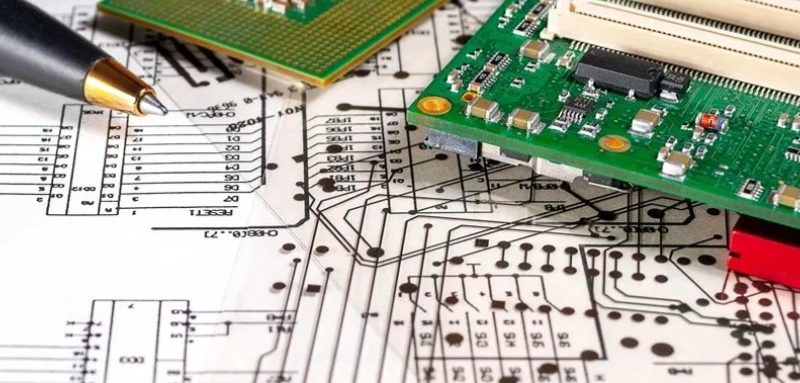
Introduction to PCB (Printed Circuit Board)
A Printed Circuit Board (PCB) is the backbone of almost all electronic devices, from household appliances to high-performance computers and smartphones. PCBs provide mechanical support and electrical connections for electronic components using conductive pathways, tracks, and pads etched from copper sheets laminated onto a non-conductive substrate.
Types of PCBs
PCBs can be classified into three main categories:
- Single-layer PCBs – Components are mounted on one side, and conductive traces are on the other.
- Double-layer PCBs – Conductive layers on both sides, connected by vias (plated-through holes).
- Multi-layer PCBs – Used in complex devices (e.g., motherboards, GPUs) with alternating signal, power, and ground layers.
PCB Design Principles
1. PCB Stackup and Layer Arrangement
Proper stackup (layer arrangement) is crucial for signal integrity and EMI reduction. Common configurations:
| 4-Layer PCB Stackup | Advantages | Disadvantages |
|---|---|---|
| Top (Signal) → GND → Power → Bottom (Signal) | Best EMI shielding, low impedance | Not ideal for high-density designs |
| Top (Signal) → Power → GND → Bottom (Signal) | Common but higher power impedance | Requires shielding for EMI |
| GND → Signal → Power → Signal | Good signal integrity | Higher power impedance |
🔹 Key Rule: Keep signal layers close to ground/power planes to reduce noise.
2. Routing and Trace Width Considerations
- Minimum Trace Width: Typically 0.2mm (8mil) for general circuits, 0.3mm (12mil) for high-density designs.
- Current Capacity:
- 1mm trace width ≈ 1A current (for 1oz copper).
- Power/Ground Traces: Wider (e.g., 80mil+) for lower resistance.
- High-Speed Signals:
- Use controlled impedance routing (microstrip/stripline).
- Keep traces short and direct to minimize delay and crosstalk.
3. Via Types and Usage
| Via Type | Description | Usage |
|---|---|---|
| Through-hole Via | Goes through all layers | General connections |
| Blind Via | Connects outer layer to inner layer | High-density designs |
| Buried Via | Connects inner layers only | Complex multi-layer PCBs |
🔹 Best Practice: Minimize via count in high-speed signals to reduce inductance.
4. Impedance Matching for Signal Integrity
- Reflections occur when impedance mismatches (e.g., trace vs. load).
- Source Termination: Add a series resistor (e.g., 33Ω for 50Ω trace) to reduce reflections.
- Differential Pairs: Maintain consistent spacing for impedance control (e.g., USB, HDMI).
5. Power and Ground Plane Design
✅ Do’s
- Use solid power/ground planes for low impedance.
- Place decoupling capacitors near ICs (e.g., 0.1µF ceramic + 10µF electrolytic).
- Keep digital & analog grounds separate (connected at a single point).
❌ Don’ts
- Avoid loops in ground traces (can cause noise).
- Don’t split ground planes unnecessarily (increases EMI).
6. High-Speed PCB Design Considerations
- When is a PCB “High-Speed”?
- Signal rise/fall time < 3x propagation delay.
- Example: A 1ns edge on a 6-inch trace requires controlled impedance.
- Critical Rules:
- Use short, straight traces for clocks & high-speed signals.
- Avoid 90° angles (use 45° or curved traces).
- Implement proper termination (series/parallel resistors).
PCB Manufacturing Process Overview
- Design & Film Printing → 2. Copper Etching → 3. Layer Lamination → 4. Drilling & Plating → 5. Solder Mask & Silkscreen → 6. Testing & Final Inspection
🔹 Common Defects: Poor copper adhesion, misaligned vias, solder mask errors.
Conclusion: Best Practices for PCB Design
✔ Plan stackup early (4-layer+ for complex designs). ✔ Route critical signals first (clocks, high-speed lines). ✔ Use proper trace widths based on current needs. ✔ Minimize EMI with solid ground planes & decoupling caps. ✔ Verify impedance in high-speed designs.
By following these PCB design principles, you can ensure better signal integrity, lower noise, and higher reliability in your electronic products.
Need Professional PCB Design Help?
🛠️ Contact us for custom PCB layouts, DFM checks, and high-speed design optimization!
