
Printed Circuit Boards (PCBs) are the foundation of modern electronics, enabling the functionality of devices from smartphones to medical equipment. This guide covers everything from PCB basics to advanced manufacturing and testing techniques.
1. What is a PCB?
A Printed Circuit Board (PCB) is a laminated structure that mechanically supports and electrically connects electronic components using conductive traces, pads, and vias etched from copper sheets. PCBs are essential in nearly all electronic devices, providing reliability and efficiency in circuit design.
-
Key Functions:
-
Mechanical support for components
-
Electrical connections between components
-
Signal and power distribution
-
2. Gerber Files for PCB Manufacturing
Gerber files are the industry-standard format used to communicate PCB design details to manufacturers. They define copper layers, solder masks, silkscreen, and drill holes.
-
Why Gerber Files Matter:
-
Ensure accurate PCB fabrication
-
Reduce manufacturing errors
-
Include layers for copper, solder mask, silkscreen, and drill data
-
3. PCB Layer Stackup Design Principles
A well-designed PCB stackup ensures signal integrity, power distribution, and electromagnetic compatibility (EMC).
-
Common Stackups:
-
2-Layer: Simple designs (low-cost)
-
4-Layer: Signal-Ground-Power-Signal (better EMI control)
-
6+ Layers: High-speed & complex designs (RF, high-frequency)
-
-
Best Practices:
-
Place ground planes adjacent to signal layers
-
Use symmetrical stackups to prevent warping
-
Optimize dielectric materials for impedance control
-
4. PCB Material Properties
Choosing the right PCB material affects performance, thermal management, and reliability.
| Material | Properties | Applications |
|---|---|---|
| FR-4 | Cost-effective, good insulation | Consumer electronics |
| Polyimide | High heat resistance, flexible | Aerospace, medical devices |
| Rogers (RF) | Low signal loss, high frequency | 5G, radar, wireless comms |
| Metal Core | Excellent heat dissipation | LED lighting, power electronics |
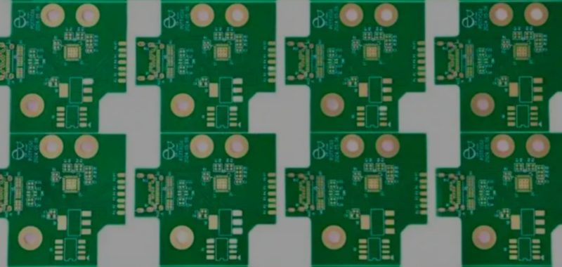
5. PCB Panelization Guide
Panelization arranges multiple PCBs into a single panel for efficient manufacturing.
-
Benefits:
-
Reduces production costs
-
Speeds up assembly (SMT process)
-
Minimizes material waste
-
-
Methods:
-
V-Score: Partial cuts for easy separation
-
Tab Routing: Small tabs hold boards together
-
Perforated Breakaways: Micro-perforations for snapping apart
-
6. Curved PCBs: Types, Structures, and Applications
Curved (Flex & Rigid-Flex) PCBs enable 3D circuit integration in compact spaces.
-
Types:
-
Flexible PCBs (FPC): Bendable (wearables, foldable phones)
-
Rigid-Flex PCBs: Combines rigid and flexible sections (medical, military)
-
-
Applications:
-
Foldable smartphones
-
Wearable health monitors
-
Automotive sensors
-
7. Types of PCBs
By Material:
-
Rigid PCBs (FR-4, Ceramic)
-
Flexible PCBs (Polyimide)
-
Rigid-Flex PCBs (Hybrid)
By Layer Count:
-
Single-Sided (1 conductive layer)
-
Double-Sided (2 conductive layers)
-
Multilayer (4+ layers, high-density)
Specialized PCBs:
-
High-Frequency PCBs (5G, RF)
-
HDI PCBs (High-Density Interconnect)
-
Metal Core PCBs (LED, power electronics)
8. PCB Design Best Practices
-
Use EDA Tools: Altium, KiCad, Eagle
-
Signal Integrity: Proper trace width, impedance matching
-
EMC Compliance: Shielding, grounding techniques
-
Thermal Management: Heat sinks, thermal vias
9. PCB Manufacturing Process
-
Design & Gerber File Generation
-
Material Selection & Cutting
-
Drilling & Plating
-
Copper Etching & Patterning
-
Solder Mask & Silkscreen Application
-
Surface Finish (HASL, ENIG, OSP)
-
Testing & Quality Control
10. 7 Essential PCB Testing Methods
-
Flying Probe Test – Checks open/short circuits
-
In-Circuit Test (ICT) – Validates component functionality
-
Functional Circuit Test (FCT) – Verifies board operation
-
Automated Optical Inspection (AOI) – Detects assembly defects
-
Aging Test (Burn-In) – Stress-tests under high load
-
X-Ray Inspection – Examines hidden solder joints (BGA)
-
Manual Visual Inspection (MVI) – Final human quality check
11. Automotive PCBs vs. Regular PCBs
| Feature | Automotive PCBs | Regular PCBs |
|---|---|---|
| Material | High-Tg, thermal-resistant | Standard FR-4 |
| Reliability | IPC-A-600 Class 3 (high-reliability) | IPC Class 2 (consumer-grade) |
| Testing | Harsh environment tests (vibration, thermal cycling) | Standard electrical tests |
12. PCBs in Medical Devices
-
Applications: MRI machines, pacemakers, glucose monitors
-
Requirements: High reliability, biocompatibility, miniaturization
13. Flexible PCBs vs Rigid PCBs
| Aspect | Flexible PCBs | Rigid PCBs |
|---|---|---|
| Material | Polyimide (PI), PET | FR-4, Ceramic |
| Cost | Higher (specialized process) | Lower (standardized) |
| Applications | Wearables, foldable devices | Computers, home appliances |
14. The difference between PCB vs PCBA
-
PCB: Bare board (no components)
-
PCBA: Assembled PCB with soldered components
15. How to Choose a PCB Manufacturer in Shenzhen
-
Check Certifications: ISO 9001, IPC, UL
-
Evaluate Capabilities: HDI, flex, high-frequency PCBs
-
Quality Control: Testing methods (AOI, ICT, X-Ray)
-
Customer Support: DFM feedback, lead times
Conclusion: Future Trends in PCB Technology
Embedded passives, 3D-printed electronics, and ultra-HDI (15μm lines) will dominate next-gen PCB innovation. Partner with AS9100-certified manufacturers for aerospace/Industrial projects.
Need PCB Design Consultation? Contact us for signal integrity analysis and DFM optimization.
Recent Comments