
Table of Contents
ToggleIf you open an X-ray of a Ball Grid Array (BGA) and see dark, circular shadows under the solder balls, you are looking at BGA voiding. While a certain level of voiding is unavoidable due to flux outgassing, excessive voids can severely compromise thermal and electrical reliability. At Fuxin PCBA, we see this issue frequently—and the solution is rarely as simple as “turning up the reflow oven.” This article explains how to investigate hidden solder-joint voids, choose practical process trials, and evaluate results against your assembly requirements.
What Causes BGA Solder Voids?
What is a BGA void? It is a cavity trapped inside the solder joint during solidification. The most common mechanism is flux material becoming trapped during joint formation, releasing vapor that cannot escape before the solder solidifies. Oxidation, flux chemistry, and the heating sequence all influence this process.
Mixed-alloy assembly deserves particular attention. Combining tin-lead solder balls with lead-free paste changes melting behavior and can trap flux. Therefore, a reflow profile proven for one combination should not automatically be applied to another.
To start the investigation, record these details before touching any machine settings:
- Package ball alloy and paste alloy.
- Flux chemistry system.
- PCB surface finish (e.g., ENIG, HASG).
- Assembly history and storage conditions.
Keep the original X-ray images alongside this record. This gives your team a defined starting point instead of guessing.
How Should You Measure and Judge Voiding?
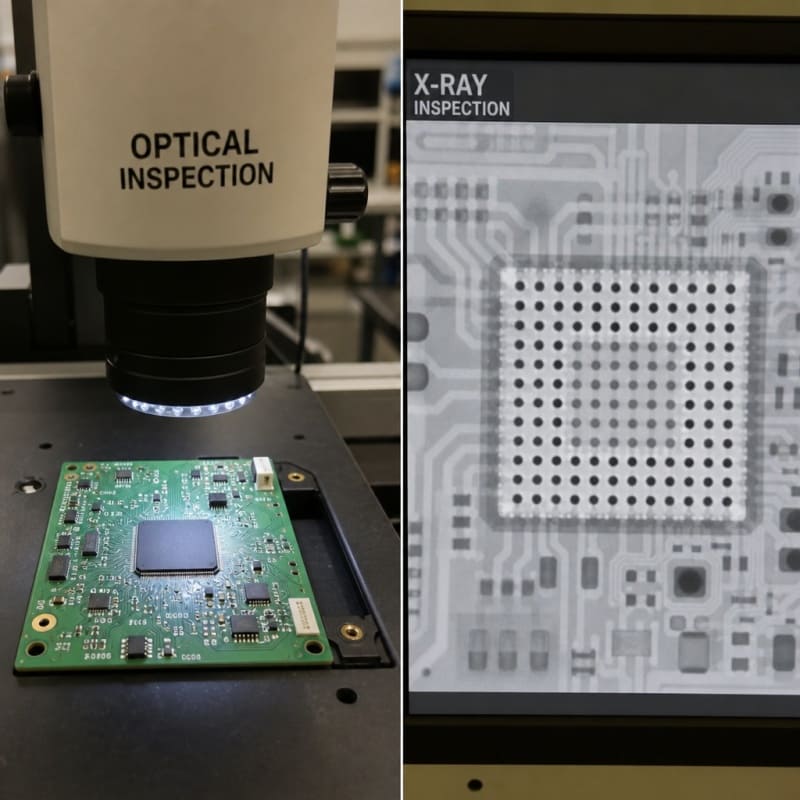
How to judge if a void is acceptable? Do not rely on a random percentage you found online. Because BGA joints are hidden beneath the package, external visual inspection cannot characterize internal cavities. You must use X-ray inspection.
Agree on the reporting method before comparing trials:
- Measurement basis: Is the result projected void area or another metric?
- Joint identification: Record the package reference, ball position, and board serial number.
- Image settings: Use a consistent X-ray inspection recipe.
- Decision criteria: Identify the governing specification (like IPC-7095) and any customer exceptions.
Remember: A measurement change should not be mistaken for a process improvement.
How to Match Solder Paste and Control Printing
Why does paste selection matter so much? Paste chemistry and flux activation directly affect outgassing. Ask your paste supplier for a “low-voiding” formulation and a recommended starting profile. However, a product described as low-voiding still needs validation on your specific board.
Before adjusting the reflow oven, verify your printing process. A reflow experiment is useless if the paste deposition is inconsistent.
Use this printing checklist during troubleshooting:
- Compare deposited paste volume across affected and unaffected BGA locations.
- Review stencil cleanliness, alignment, and aperture condition.
- Check whether deposits remain consistent after production pauses.
- Record printer settings and stencil revision with each trial.
Avoid a blanket instruction to “print less paste.” Instead, define a specific aperture change and inspect the resulting joints. Your goal is a controlled deposit that meets joint requirements.
Why Can a Hotter Reflow Profile Make Matters Worse?
Why not just crank up the heat? Because successful reflow depends on the timing of flux activity and wetting, not just peak temperature. Inappropriate heating can dry out the paste, impair wetting, and actually increase oxidation and voiding.
How to tune the profile correctly?
- Measure the actual board, not just the oven setpoints. Use thermocouples to record the thermal response at the BGA ball locations.
- Combine the paste supplier’s process window with the component’s temperature limits.
- Treat soak duration, heating rate, and time above liquidus as trial variables. A longer soak is not automatically better; it depends on your specific paste and board mass.
Review Pad Design and Via Construction
If voiding repeatedly happens at the same pad locations, look at the PCB design. Uncapped vias under the BGA pads can contribute to trapped air and outgassing during reflow.
Ask your PCB designer and fabricator to review the affected locations together. Key questions to ask:
- Do vias intersect the solder lands?
- Are those vias filled and capped (VIP) or left open?
- Does the fabrication drawing clearly specify the intended via construction?
Document any proposed design change before ordering another board revision. This connects a design correction directly to an observed problem.
How to Run a Controlled Voiding Reduction Trial
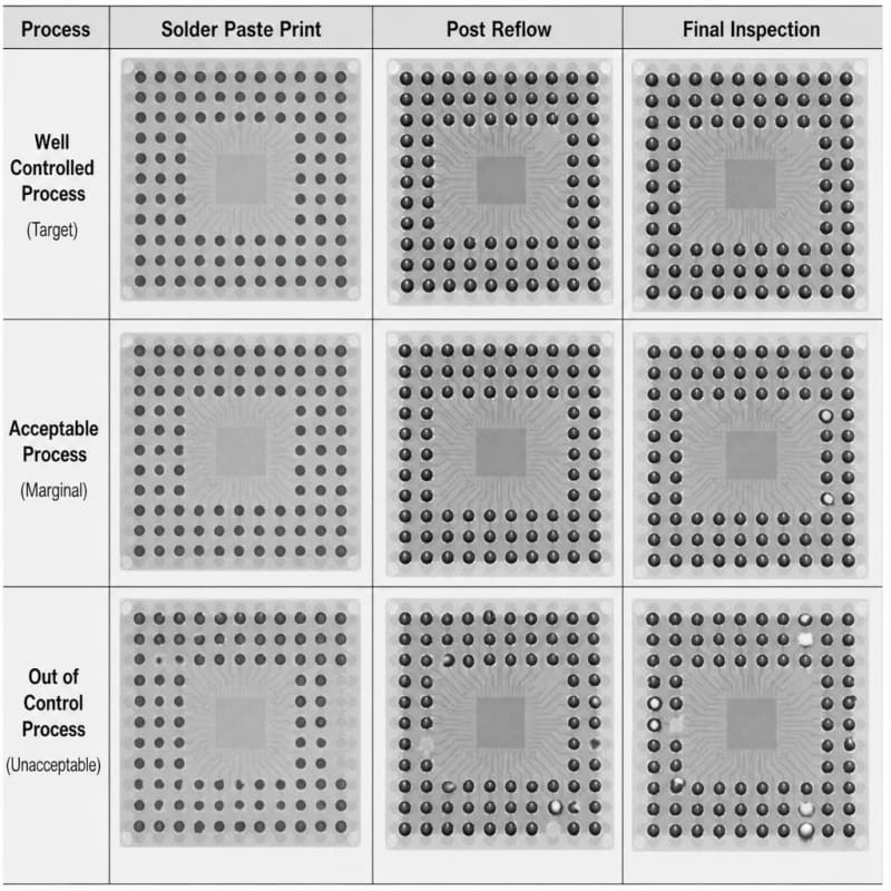
A documented experiment is far more useful than several simultaneous adjustments. Here is a practical sequence:
- Capture the baseline: Save X-ray results, printing records, and the measured profile.
- Choose the first variable: Compare a profile adjustment or a candidate paste while holding other conditions stable.
- Define success beforehand: Include voiding results, other joint-quality requirements, and repeatability.
- Repeat promising conditions: Verify the result survives another run.
- Release deliberately: Update work instructions, inspection settings, and change-control records together.
Build a Repeatable Process, Not a Better-Looking Sample
The practical takeaway is to define acceptance, measure consistently, and test a clear hypothesis before changing production. Keep paste, printing, thermal profiling, and PCB construction in the same investigation.
When evaluating PCBA Contract Manufacturing support, ask how the supplier would investigate your specific assembly rather than requesting a generic promise of zero voids. Prepare your design files, BOM, package information, and existing X-ray images, and ask for a written trial plan with deliverables.
Frequently Asked Questions
There is no universal number. Acceptance criteria depend on the IPC class (e.g., IPC-7095), the thermal demands of the specific component, and the end-use environment. Always agree on the measurement method and limits before production.
Yes. Excessive voids can reduce thermal conductivity, causing the BGA to overheat. They can also reduce mechanical strength, leading to cracks under thermal cycling or vibration.
Not necessarily. While a properly tuned soak can help flux activate and gases escape, an excessively long soak can dry out the paste, impair wetting, and actually increase voiding. It must be tested with your specific paste and board.
Only X-ray inspection (2D or 3D) can reveal hidden voids under BGA packages. 3D X-ray (CT scanning) provides the most accurate volumetric data for critical assemblies.
Yes. Our engineering team can review your X-ray images and process data to identify root causes—whether it’s paste selection, stencil design, or PCB via construction.
Start Your PCBA Inquiry Today
Prepare a focused inquiry with your project stage, required quantity, and current documentation. Highlight your main constraint, whether that is an unresolved component or a strict delivery target.
Explore our broader PCB Assembly services:https://www.fuxinpcba.com/pcb-assembly/